


Thin film deposition and growth services
·Atomic layer deposition (ALD): Used for the growth of high - quality oxide and nitride thin films.
·Magnetron sputtering: Used for the physical vapor deposition of metal or compound thin films.
·Electron beam evaporation: Used for the evaporation and deposition of metals (such as Ti, Ni, Ag, Al, etc.).
·Plasma - enhanced chemical vapor deposition (PECVD): Used for the deposition of dielectric thin films such as SiO₂, SiN₃.
·Metal - organic chemical vapor deposition (MOCVD): Used for the epitaxial growth of compound semiconductors.

·Coating and developing: Supports wafers up to 8 inches in diameter or 6×6 - inch substrates.
·Photolithography (SUSS lithography machine): Supports projection - type photolithography and is suitable for wafers from 2 inches to 200mm in diameter.
·Electron beam lithography (EBL): Supports direct writing of high - resolution patterns ≤10nm.
·Plasma photoresist stripping (ashing): Used for photoresist removal.

Etching and cleaning services
·Reactive Ion Etching (RIE): Dry etching, suitable for dielectric materials.
·Inductively Coupled Plasma Etching (ICP): High - density plasma etching, suitable for SiO₂, SiN₃, etc.
·RCA Cleaning: Standard wafer cleaning process.
Water cleaning, organic ultrasonic cleaning: Suitable for 4/6 - inch wafers.
·Spin dryer: Wafer dehydration and baking.

Materials and surface analysis services
·Profilometer: Measurement of thin - film thickness and surface morphology.
·Thin - film stress tester: Measurement of substrate deformation caused by thin - film stress.
·Optical film thickness measuring instrument: Measurement of thin - film thickness through spectral reflection.
·3D optical profiler: Analysis of surface roughness and morphology.
·Atomic force microscope (AFM): Analysis of nanoscale surface morphology and physical properties.
·High - resolution X - ray diffractometer (HRXRD): Analysis of crystal structure, stress, and phase.
·Scanning near - field optical microscope and Raman system: Analysis of chemical composition, crystallinity, and morphology.
·Photoluminescence test (PL): Analysis of material energy bands and defects.
·Transmission electron microscope (TEM): Analysis of surface morphology and composition (Need to confirm availability).
Electrical and device testing services
·Fully automatic probe station and test system: Suitable for two·Semiconductor parameter test system: I-V, C-V, pulse test, etc.
·Power device static parameter test system: On-resistance, threshold voltage, breakdown voltage, etc.
·Dynamic parameter test system: Switching characteristics, reverse recovery, gate charge, etc.
·Thermal characteristic test system: Junction-to-case thermal resistance, heat capacity, thermal conductivity, etc.
·Variable temperature Hall test system: Measurement of carrier concentration, mobility, resistivity.
·Emission Microscope (EMMI): Defect location and leakage analysis.
Post - processing and packaging related services
·Wafer thinning: Suitable for 4/6-inch silicon carbide wafers.
·Laser dicing: High-precision wafer cutting.
·Marking machine: Laser marking on wafers.
·Rapid thermal annealer: Wafer annealing treatment.
·Graphite carrier disk baking: Used for post - processing of MOCVD.
Other special services
·Focused Ion Beam (FIB): Fixed-point cutting and cross - section analysis.
·Radio Frequency Glow Discharge Spectrometer: Element analysis and depth profiling.
·High - current ion implantation: Used for doping of SiC power devices.


Contact us
Tell us your needs

Materials based on customer needs
Scheme planning, functional design, and technical feasibility assessment

Cost estimation
Prepare pre - sales documents
 、
Customer communication and demonstration
Finalization of the plan
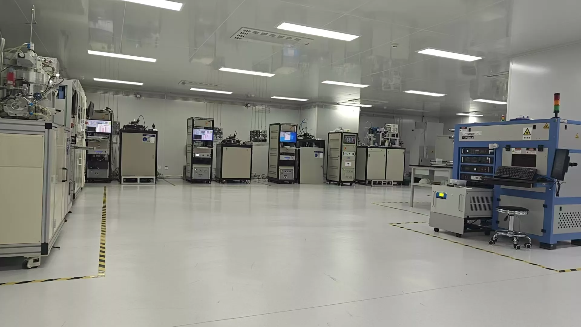
At Progressive Semiconductor, we offer a full - process service covering epitaxial growth, chip manufacturing, packaging and testing,41 kinds of advanced equipment leasing services, to help customers achieve their R & D and production goals in a more efficient and flexible way. Whether it's MOCVD, lithography machines, etching equipment, thin - film deposition systems, or various special machines for testing and packaging, customers can choose short - term or long - term leasing plans according to the project cycle and actual needs, significantly reducing the initial investment and equipment maintenance costs.
All equipment has undergone strict calibration and regular maintenance to ensure stable and reliable performance; the professional engineer team also provides one - stop technical services from equipment configuration, operation training to process support, ensuring that customers can easily connect and quickly start production. Choosing Progressive Semiconductor equipment leasing means that you can flexibly access industry - leading process resources at a lower cost and with a lighter asset structure, and efficiently promote the project progress.

Have technology
Development History


友情链接:西安电子大学芜湖研究院 hpmc manufacturer