[Popular Science] Introduction to Enhanced HEMT Devices

2024-05-08 10:21
With the continuous improvement of power density and operating frequency of power conversion systems , need to develop performance better thanTraditional semiconductor power devicesGaN (GaN) as a typical representative of the third generation of semiconductor materials , is considered to be a way to improve the conversion efficiency of high-power power systems.The main candidate material for the next generation of power devices with high efficiency. , enhanced (also known asNormally closed) device has a safety , can simplify electricalAdvantages such as circuit design and better circuit topology design , which is more attractive in industrial applications.Enhanced-mode HEMT.
at present , in the third generation and a halfConductor material , GaN( GaN) and silicon carbide ( SiC) The development ofMature , and the material itself has a large critical breakdown electric field , high temperature resistance andAnti-radiation and other characteristics , so it is more suitable for making power electronic devices。 eyeforward,SiCAt high voltage (above 1200 V) Market shareObvious advantages , but inPower conversion and high frequency operation,GaNHas more obvious advantagesMomentum 。GaN The converter's low losses are due to its low switching losses ,thisIt is becauseGaNCompared toSiC Has better electron transmission ability.HereThe structure of epitaxial growth in the plane direction has strong spontaneous polarization and compressiveElectric polarization effect , which will lead toGaNHeterojunction structure of materials (typicallyTypeAlGaN/GaN) A high concentration of two-dimensional electron gas is generated at the interface(2YOU),thereforeGaN The device has lower on-resistance.At the same voltage rating ,GaN MaterialsSuitable for As efficient power electronic devices , especially the high electron transfer of lateral structures Shift transistor (ALL), its on-resistance ratioAnd The device's on-state Low resistance 1~2 orders of magnitude , and the third generation semiconductor materialsSiC Device comparison , its on-resistance is reduced by 1/2~ 1/3。
From the perspective of device structure,GaNThe device is divided into vertical and horizontal structures 。Vertical structure devices need to use GaNFree-standing substrate , and currentlyComelook ,GaNThe cost of self-supporting epitaxial wafers is high, andGaNSelf-supporting liningThe epitaxial wafer size is smaller, which makes the cost of a single device higher.high Horizontal devices from the perspective of switch type , divided intoDepletion type (normally open) ,D-mode) and enhanced (normally closed ,AND-mode) Device.AlGaN/GaN The interface will produce a high electron concentration (about 1013 cm -2 .eV -1),high Migration [ About 2000 cm2/( V .s) ]of2YOU , traditionalGaN ALLIt is depletion type , that is, the device gate is There is still a high concentration of 2YOU , so that the deviceIn open state . However, the enhancement mode device can be depleted at zero gate bias. In the channel below the gate 2YOU , putting the device in the off state. Therefore, the device has the advantages of safety, energy saving and simplified circuit design. Advantages , which is an important development direction of future power devices.
From the perspective of market application , with a withstand voltage of 600~ 1200 V boundary , less than 600 V The market GaN Main , mainly for consumerElectronics , this is currentlyGaN The most important breakthrough in material entry into the marketmouth 。600~ 1200 V This range isGaN and SiC Areas of coexistence ,   Its main application is in electric vehicles ( THIS) and hybrid electric vehicles ( TOGETHER)Converters and inverters for renewable energy sources. Above 1200 V ofMarket SiC Main ,futureGaN If the crystal quality of the material can be further improved The defect density of the bulk material is further reduced, or the longitudinal structureofGaN Improved device technology maturity , which will also be in the high voltage marketDemonstrate stronger competitiveness 。
fromFrom basic research to industrialization , there are several important indicators to evaluateGaNEnhanced ALLDevice performance ,Typical breakdown voltage InB,thresholdValue voltage Inth, on-state resistance Ron, saturation current density IDS, gate withstand voltage, thresholdVoltage hysteresis, etc. This paper reviews the implementation of a series of enhancement mode devicesplan , focusing on the power device technology based on gate groove structureand several important processes , and proposed possible technical solutions for the future.
Depletion mode ALLDevice:
Due to the depletion mode The gate of HEMT devices does not require complex special processing, so the device technology matures early. With the continuous improvement of the manufacturing process, key parameters such as the device's on-current, breakdown voltage, and characteristic resistance have achieved relatively ideal results.
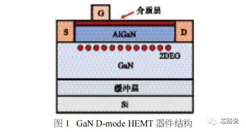
GaN D-mode HEMTDevice structure: depletion type The reliability issues faced by GaN HEMT in the industry mainly include current collapse and threshold voltage drift in hard switching mode., These reliability issues are related toThe design of the field plate, the selection of the gate dielectric layer, the design of the GaN buffer layer and the selection of the passivation layer material are related.The manufacturing process details of the device need to be further optimized to improve the reliability of the device.

图片

Enhanced HEMT devices:
Enhanced There are several methods for operating GaN HEMT devices, mainly based on depleting/weakening the polarization charge at the AlGaN/GaN heterojunction interface.
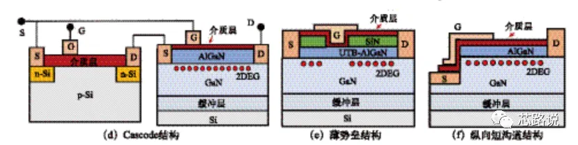
Several mainstream schemes for achieving enhancement mode operation include recessed gate structure, fluorinated gate structure and In addition, the cascode structure, the UTB structure, and the vertical short-channel VG-HEMT structure can also achieve enhanced operation of the device.

图片

The etching of the gate barrier layer often introduces interface states, which adversely affects the performance of the device. At the same time, the control of etching accuracy will also affect the device. threshold voltage and on-resistance.
The recessed gate structure generally uses a metal-insulator-semiconductor (MIS)/metal-oxide-semiconductor (MOS) structure, which enables the device gate to have a larger safe operating range and lower leakage current.However The threshold voltage stability of MIS/MOS devices is poor, primarily due to charges and traps at the dielectric/semiconductor interface. Reports indicate a high interface trap density (Dit) at the oxide/III-nitride interface, leading to increased gate leakage current and unstable threshold voltage. Therefore, the interface states of the gate trench and the quality of the dielectric layer are crucial factors in the pursuit of high-performance GaN HEMT devices.
based on Enhancement-mode HEMT devices with p-GaN insertion layer structure,The p-GaN insertion layer structure is also a solution to achieve enhanced operation of HEMT devices.The advantage of this structure is that it can eliminate the influence of the gate dielectric layer on the device, but its typical disadvantage comes from the pn junction formed by p-GaN and the AlGaN underneath. This pn junction will turn on in the forward direction when the positive voltage applied to the gate exceeds a certain threshold, thereby increasing the gate current and causing device failure.
Based on the enhanced device of cascode structure, cascade technology is an important technical route to achieve enhanced operation.It connects a Si MOS transistor and a depletion-mode GaN-based HEMT in a cascode configuration. The external D terminal of the device serves as the drain of the HEMT, the external S terminal serves as the source and gate of the MOS transistor, and the external G terminal serves as the gate of the MOS transistor. The drain of the MOS transistor is connected to the source of the HEMT. When the voltage applied to the G terminal exceeds the threshold voltage of the MOS transistor, the MOS transistor conducts, generating a large current at its source and drain terminals, and the voltage drop across the terminals is negligible. This also means that the voltages at the source and gate terminals of the HEMT are approximately equal, meaning the gate voltage is 0 V, and the depletion-mode HEMT conducts. Therefore, any electrical signal applied to the D terminal of the device generates a current, which flows through the series circuit of the HEMT and MOS transistor, turning the entire device on. Similarly, when the voltage applied to the G terminal is less than the threshold voltage of the MOS transistor, the MOS transistor is turned off, and a large voltage drop occurs at its source and drain terminals. The voltage difference between the source and gate terminals of the HEMT is also obvious. The gate voltage in the HEMT is less than the threshold voltage and less than 0V. The depletion-mode HEMT is turned off, and the entire circuit connected in series with the HEMT and MOS transistor is shut down.
The advantage of cascading technology is that it bypasses the enhanced The technical difficulty of HEMTs lies in achieving enhancement-mode operation using Si-based MOS transistors, a technology that is currently highly mature. In theory, the gate drive required for cascode transistors is the same as for traditional Si MOS transistors, simplifying the design of additional drive circuits. However, the disadvantages of cascode technology are also significant. It increases the complexity of subsequent packaging technology. At high temperatures, the device is still limited by the performance of Si transistors, making the advantages of GaN-based HEMTs difficult to realize. The unique connection method of the two transistors forms an internal circuit in the cascode device, increasing the device's internal parasitic inductance. Due to the low electron mobility of Si transistors, cascode transistors are difficult to use in high-frequency applications above 1 MHz.
Other enhancement mode device solutions, such as fluorinated gate structure enhancement mode A key feature of HEMTs is the ion implantation of fluorine ions into the gate barrier layer. Furthermore, the VG-HEMT structure also enables enhancement-mode operation of HEMT devices. This is achieved by converting a portion of the device channel into a longitudinal configuration. Since this longitudinal portion lacks a 2DEG, the device remains in the off state at zero gate bias.END
(Note: The text is for technical communication only and aims to promote industry progress. The pictures are from the literature.)
Editor: Xin Lu
AND-mail:hsglb2005@163.com
Reference: Huang Huolin"GaN"Base EnhancedALLDevice research progress." Electronics and Packaging23(1). (2023)


email
suijiabin1993@gmail.com
whatsapp
whatsapp
whatsapp
亿鸽在线客服系统